Sony has created the world’s first 1 stacked CMOS image sensor technology with 2 Layer Transistor Pixel. Whereas photodiodes and pixel transistors in typical CMOS image sensors share the same substrate, Sony’s innovative technology divides photodiodes and pixel transistors on independent substrate layers. This innovative architecture almost doubles 2 saturation signal level 3 compared to traditional image sensors, broadens dynamic range, and decreases noise, resulting in significantly improved imaging qualities. The pixel structure of the new technology will allow pixels to preserve or improve their present qualities at not only current but also reduced pixel sizes.
Sony made the announcement during the IEEE International Electron Devices Meeting, which began on Saturday, December 11, 2021.
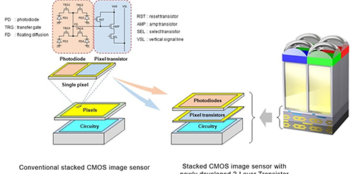
A stacked CMOS image sensor is made up of a pixel chip made up of back lit pixels layered atop a logic chip where signal processing circuits are built. Photodiodes for converting light to electrical signals and pixel transistors for regulating the signals are located on the same layer of the pixel chip. Increasing the saturation signal level within form-factor limits is critical for achieving great image quality with a broad dynamic range.
Sony’s new design represents a step forward in stacked CMOS image sensor technology. Sony placed the photodiodes and pixel transistors on separate substrates stacked one on top of the other using its unique stacking process.
In contrast, photodiodes and pixel transistors in traditional stacked CMOS image sensors are located on the same substrate. The novel stacking technique permits the use of topologies that allow for the optimization of the photodiode and pixel transistor layers, doubling the saturation signal level relative to conventional image sensors and, as a result, increasing the dynamic range.
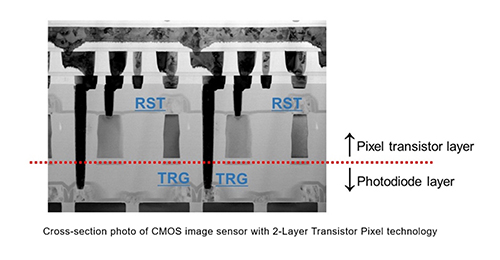
Furthermore, because pixel transistors other than transfer gates (TRG), such as reset transistors (RST), select transistors (SEL), and amp transistors (AMP), occupy a photodiode-free layer, the size of the amp transistors may be expanded. Sony was able to significantly reduce noise in nighttime and other dark-location photos by increasing the size of amp transistors. This new technology’s increased dynamic range and noise reduction will avoid underexposure and overexposure in situations with a mix of bright and dim lighting (e.g., backlit settings) and enable high-quality, low-noise photographs even in low-light (e.g., interior, nighttime) circumstances.
Sony’s 2-Layer Transistor Pixel technology will help to realise increasingly high-quality imagery, such as smartphone pictures.